Experimental Condensed Matter Physics
Clean room
Experimental Condensed Matter Physics
Clean room
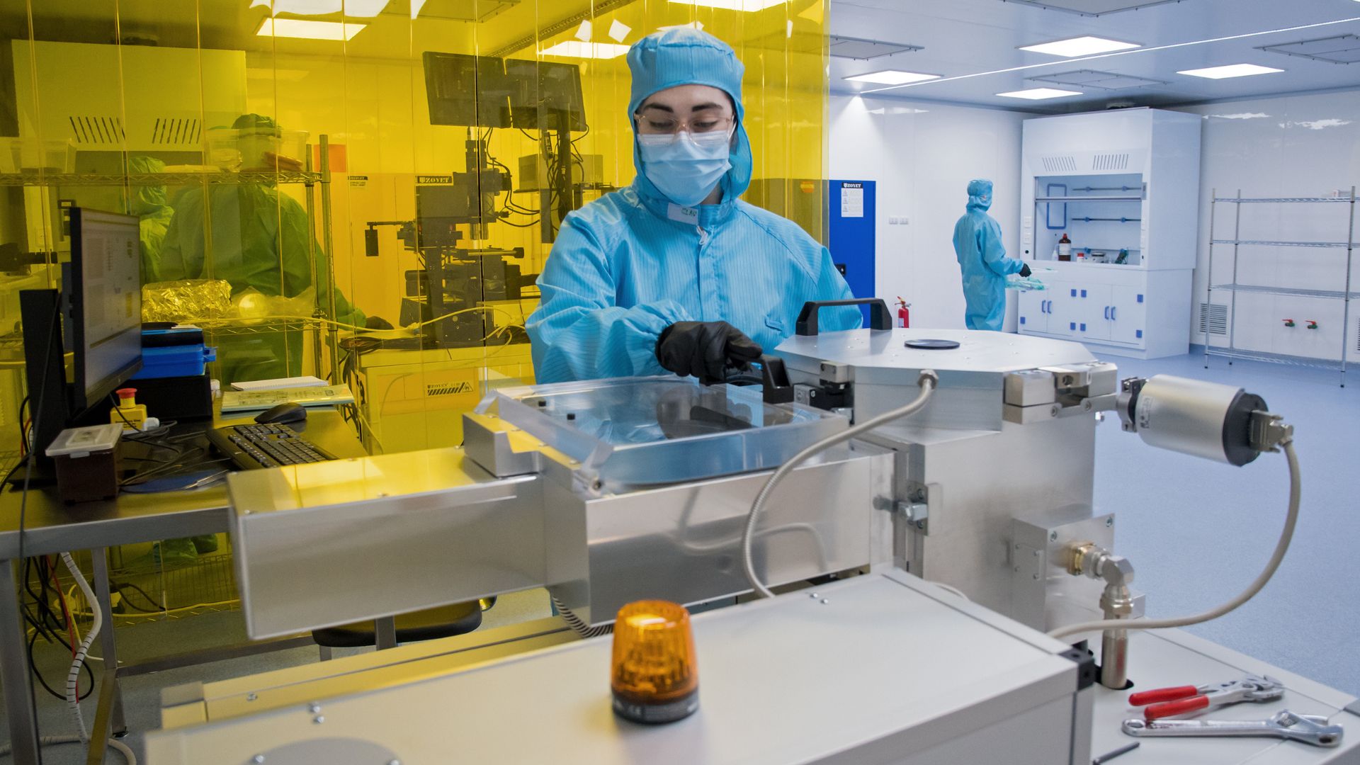
Reactive ion etching equipment (RIE)
The user works with the reactive ion etching equipment (RIE), which completes the process of etching structures with micrometric resolution through bombardment with ions (FONDEQUIP EQM190136).
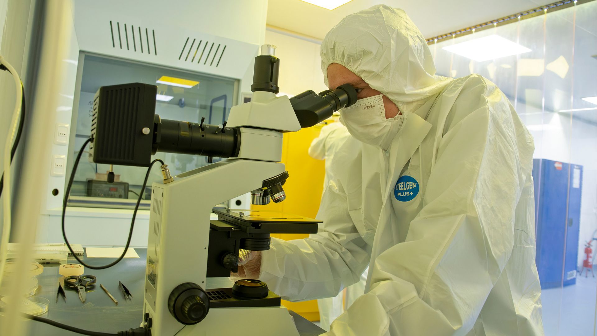
Optical microscope
The user is working with an optical microscope to verify the lithography of a silicon wafer.
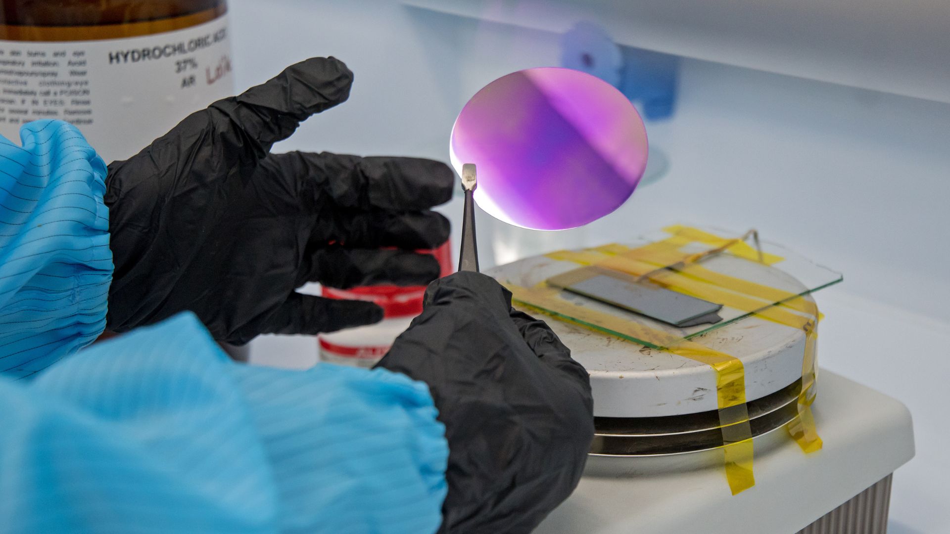
Photoresist varnish on a silicon wafer
The user finishes the coating treatment with photoresist varnish on a silicon wafer for subsequent pattern etching on the mask aligner.
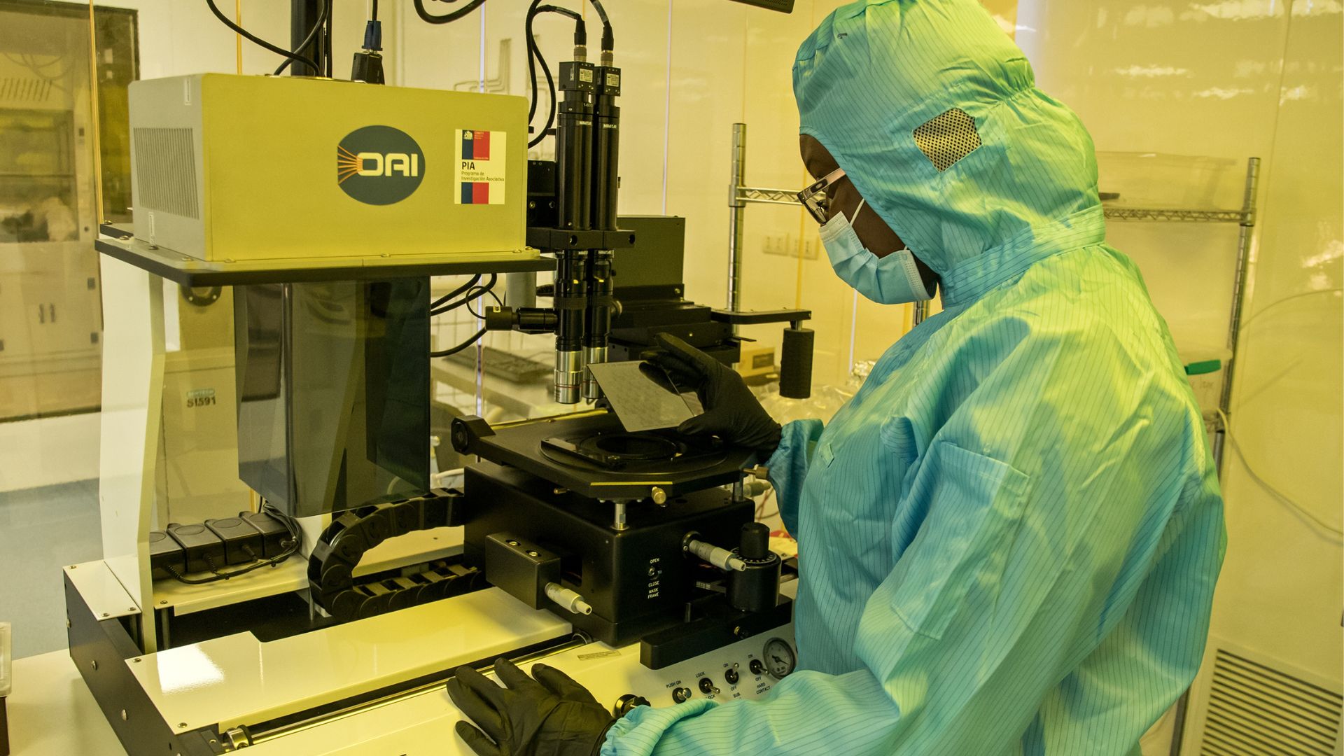
Mask aligner
The user is working with the mask aligner, drawing a pattern of micrometric structures on a silicon wafer, which the RIE will then etch.

Chamber for optical lithography
The air purity in this room is even better than the rest of the clean room since it is designed for high-resolution optical lithography.
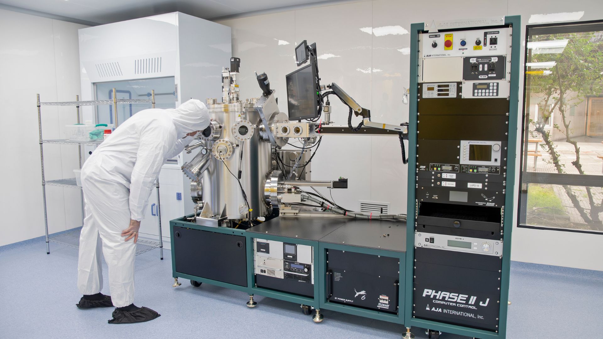
Magnetron sputtering equipment
Magnetron sputtering equipment for fabrication of thin films of nanometric thickness (FONDEQUIP EQM210105).
Welcome to the Institute of Physics Clean Room. We invite you to click on each of the highlighted points to learn more about our techniques and equipment.