This area of physics is concerned with studying the properties of the condensed phases of matter, particularly the solid and liquid states, following the principles of quantum mechanics, electromagnetism, statistical mechanics and, at the macroscopic level, thermodynamics.
There is a direct connection between theoretical and experimental discoveries in this area of physics and the consequent technological applications, mainly in the fields of microelectronics, materials engineering and, more recently, nanotechnology.
The UC Institute of Physics is a national and international benchmark in the theoretical and experimental study of condensed matter physics.
ON THIS PAGE
Description
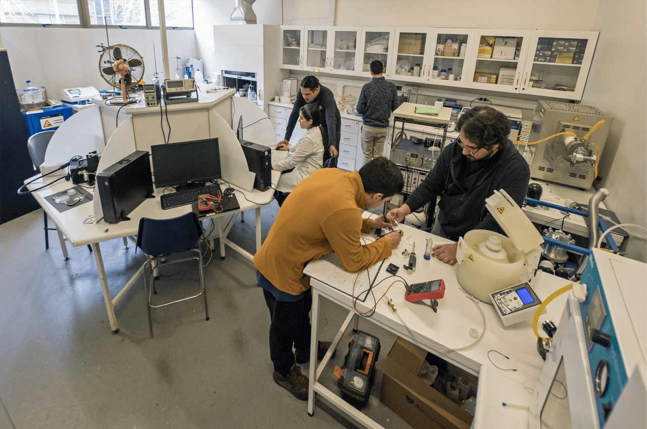
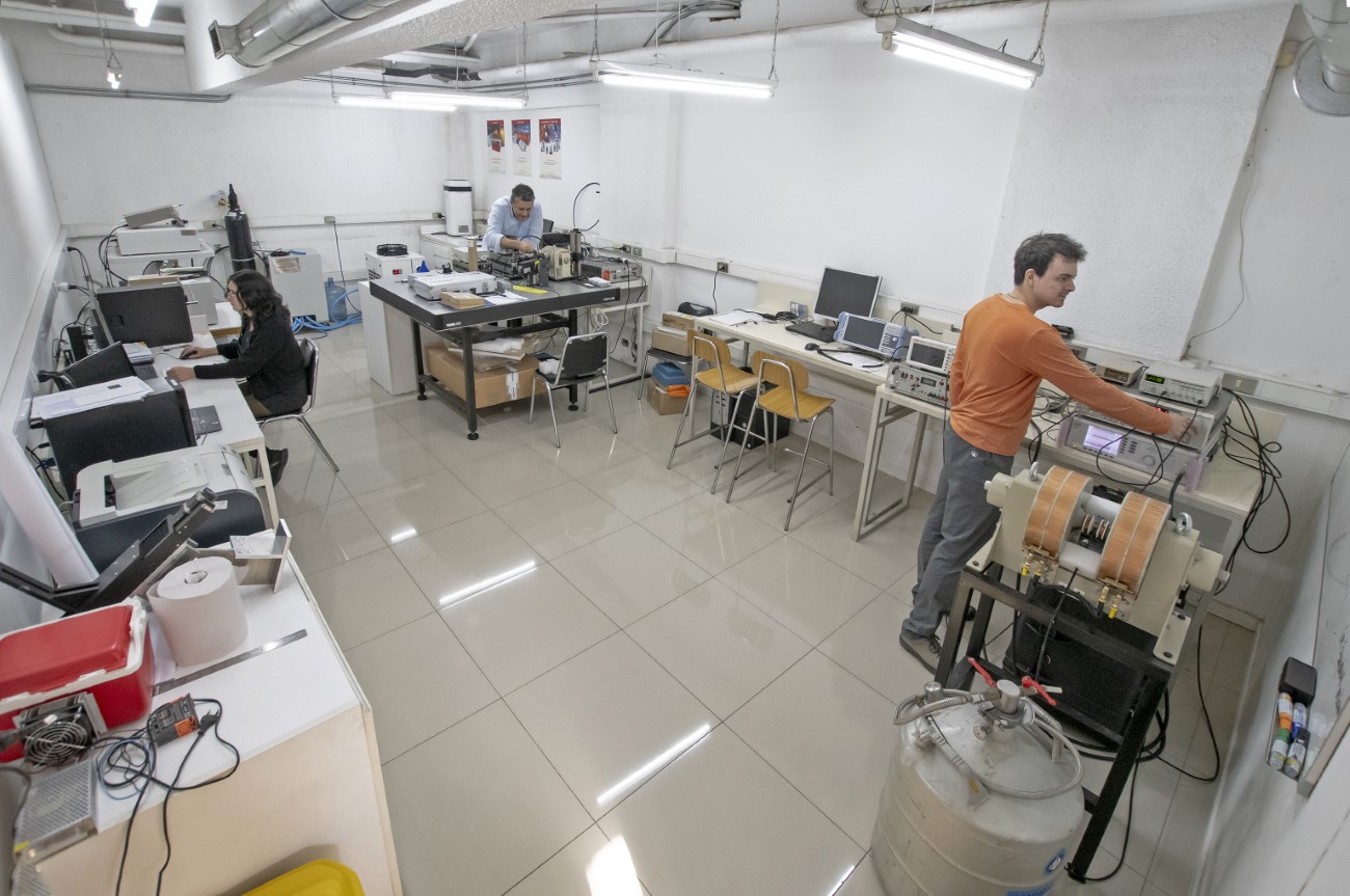
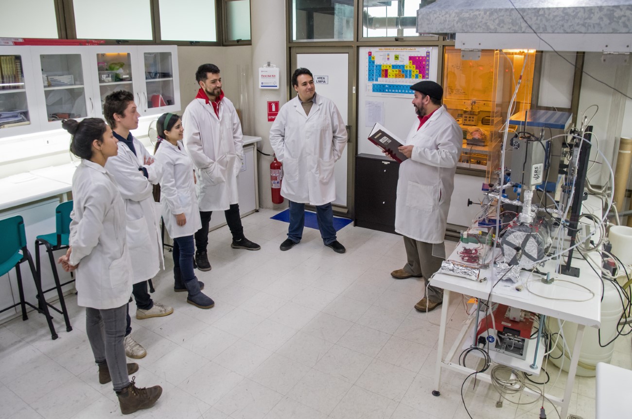
The Experimental Condensed Matter Physics Group is dedicated to the empirical investigation of micro and nanometer scale phenomena of technological importance. With this objective, several research laboratories in materials and surface science have been implemented, which have enabled the development of first rate academic publications, as well as undergraduate and graduate experimental theses.
Questions this area strives to answer
Materials and Surface Science
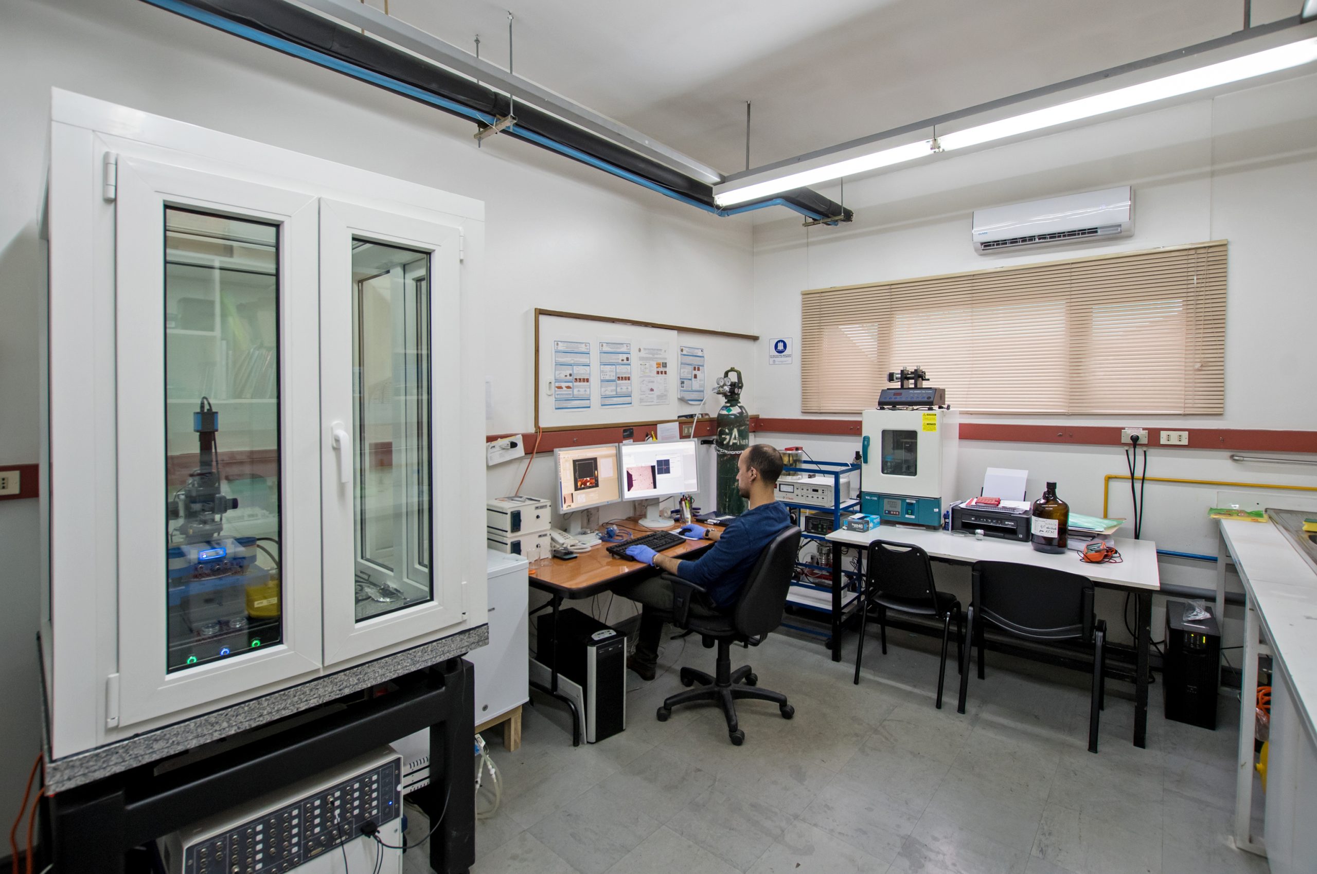
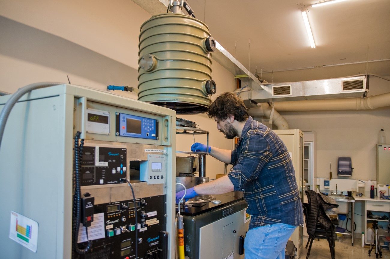
Studies involving the interaction of gases with solid surfaces of metallic, semiconductor and ferroelectric materials are carried out in the Materials Science Laboratories. These solid surfaces may be metallic foils 0.1 mm thick, thin films 20 to 500 nm thick, or nanostructures such as “dots” or “clusters” of a few atoms.
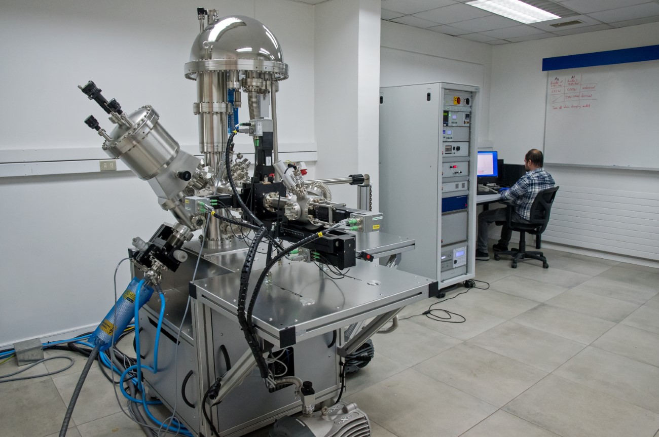
These studies could have direct applications in hydrogen storage devices, gas sensors and new electronic transducers. The investigations are carried out by measuring the changes in electrical, magnetic and optical properties when solid surfaces come into contact with certain gases such as hydrogen, carbon monoxide and carbon dioxide. Characterization of the materials is carried out using various spectroscopic techniques, including electron (Auger), x-ray dispersive analysis (EDS) and visible light (Raman).
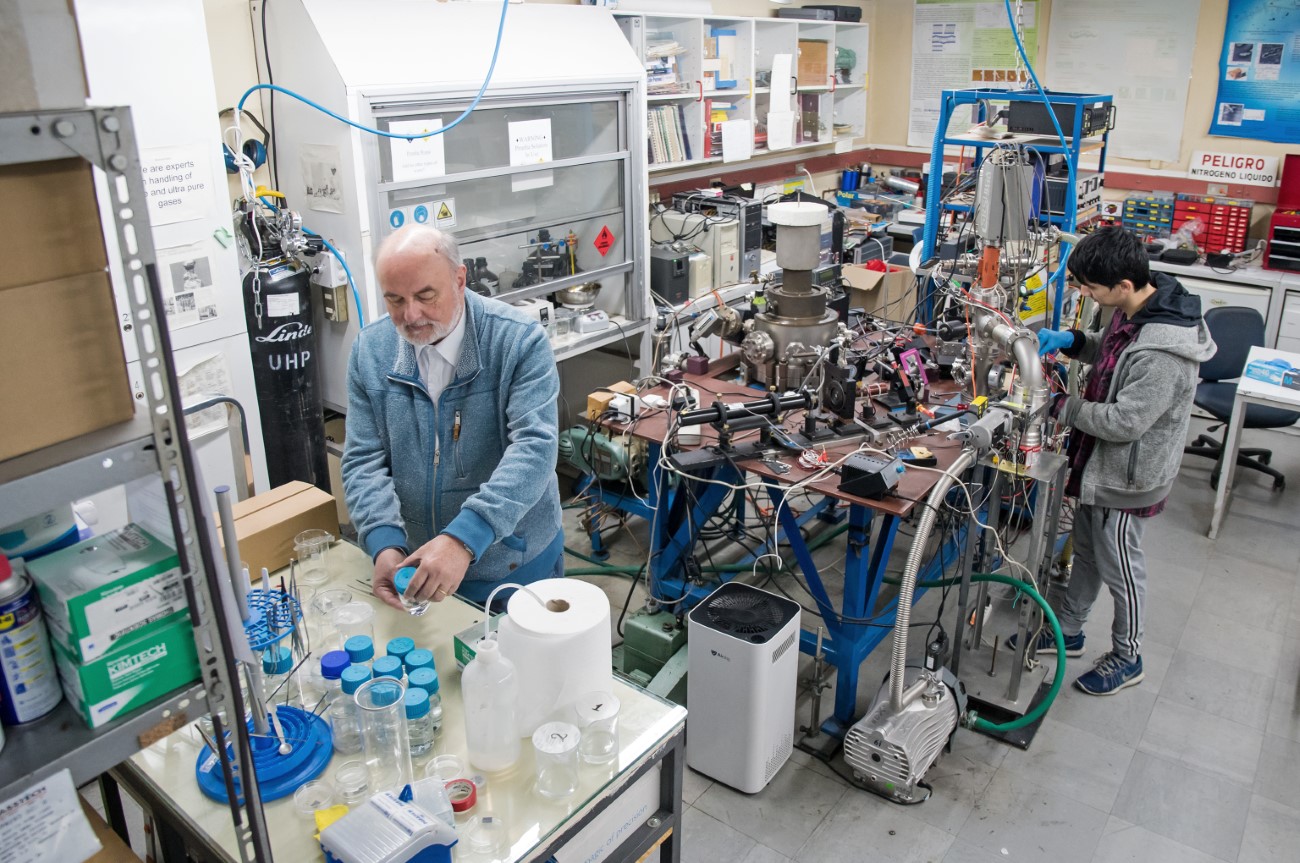
In the Laboratory for Experimental and Applied Physics of Interfaces (Surflab) the structures and dynamics of bionanomaterials, soft material films, and magnetic films are researched. One aim is to better understand the forces behind structural changes, self-assembly processes, and dynamics of films and interfaces of organic-biological and inorganic materials. Techniques such as High Resolution Ellipsometry (VHRE), Imaging Ellipsometry (IE), Atomic Force Microscopy (AFM), Magneto-Optical Kerr Effect (MOKE), and Programmed Thermal Desorption (TPD) of properly prepared films are used for such studies. All equipment is designed and manufactured in the laboratory. Instruments are continuously updated and new techniques for sample preparation and analysis are developed as required.
Nanotechnology
In the Nanotechnology subarea of the UC Institute of Physics, the physical properties of nanomaterials are studied. The fabrication of nanostructures is carried out by means of, for example, a nanoporous membrane that can be produced in a controlled manner, allowing to vary the size of its pores from 20 nm to 200 nm. It is thus possible to fabricate nanotubes, nanopillars or nanopoints of different materials, such as, for example, carbon nanotubes or magnetic nanopoints. Various microscopy or spectroscopy techniques are used to characterize these materials and study the behavior of their properties at low temperatures (a few degrees Kelvin).
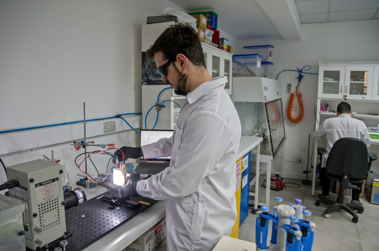
The next step is to explore how these nanomaterials can be used in different technological applications. In particular, it is possible to increase the efficiency of photocatalysts for hydrogen production by decomposing water using sunlight, as well as for use in chemical and biological sensors.
The laboratories currently located in the Hernán Chuaqui building allow the study of nanostructures and mesoporous materials of metal oxides and suboxides for applications in sensors, electro-optical devices, microbatteries, and photocells.
In particular, the relationship of growth conditions and kinetics with the morphological, chemical, and structural characteristics of the material is studied; stability experiments and thermally induced phase transitions (amorphous-crystalline) and structural transformations of metastable materials grown outside equilibrium conditions are performed. Other studies involve understanding the effect of size and microstructure of nanoparticles, thin films, and multilayers on oxidation-reduction behavior. This is fundamental to modify and control their electrical, optical, catalytic, and interface properties, crucial for the development of technological devices.
In turn, the Chemical Vapor Deposition (CVD) Laboratory, housed in a clean room, allows the fabrication of various types of multifunctional materials of technological interest including, among others, cutting tool coatings, multiferroic films, multilayers, and magnetic nanostructures. The versatility of this growth technique allows to produce and modify such materials in a controlled manner and thus take advantage of the main properties they possess. The samples produced are characterized with microscopy and spectroscopy techniques in order to guarantee the successful fabrication of each material.
Research Area
